
Characterization And Measurement Collection

Characterization and measurement play a crucial role in various scientific fields

Background imageCharacterization And Measurement Collection: X-ray crystallography C016 / 3824

X-ray crystallography C016 / 3824
X-ray crystallography. Researcher using an X-ray machine to obtain crystal diffraction patterns of proteins for 3-D imaging of enzymes

Background imageCharacterization And Measurement Collection: FE scanning electron microscopy C016 / 3821

FE scanning electron microscopy C016 / 3821
FE scanning electron microscopy. Researcher operating a field-emission scanning electron microscope (FE-SEM). This is a F JEOL 6320F FE-SEM

Background imageCharacterization And Measurement Collection: Scanning transmission electron microscopy C016 / 3815

Scanning transmission electron microscopy C016 / 3815
Scanning transmission electron microscopy. Researcher using a scanning transmission electron microscope (STEM) to analyse the structure of solid-state materials

Background imageCharacterization And Measurement Collection: Rutherford backscattering spectrometer C016 / 3834

Rutherford backscattering spectrometer C016 / 3834
Rutherford backscattering spectrometer chamber. This is a view of the inside of one of the chambers of the spectrometer. Rutherford backscattering spectroscopy (RBS)

Background imageCharacterization And Measurement Collection: Nuclear magnetic resonance spectrometer C016 / 3830

Nuclear magnetic resonance spectrometer C016 / 3830
Nuclear magnetic resonance (NMR) spectrometer. NMR spectroscopy measures the resonance between an applied magnetic field and the magnetic moment of a molecules atoms

Background imageCharacterization And Measurement Collection: Pulse laser deposition apparatus C016 / 3828

Pulse laser deposition apparatus C016 / 3828
Pulse laser deposition apparatus. Close-up of the sample holder of a pulse laser (blue light) being used to deposit material on the surface of a photovoltaic cell

Background imageCharacterization And Measurement Collection: Photovoltaic cell testing C016 / 3829

Photovoltaic cell testing C016 / 3829
Photovoltaic cell testing. Set-up for an I-V (current-voltage) test stand for testing of a photovoltaic cell. This is a point contact configuration for the apparatus

Background imageCharacterization And Measurement Collection: Molecular beam mass spectrometer C016 / 3825

Molecular beam mass spectrometer C016 / 3825
Molecular beam mass spectrometer (MBMS). This machine is being used to analyse vapours during gasification and pyrolysis processes in research into the thermochemical conversion of renewable energy

Background imageCharacterization And Measurement Collection: Silicon cluster manufacturing tool C016 / 3822

Silicon cluster manufacturing tool C016 / 3822
Silicon cluster manufacturing tool. Technician working on a silicon cluster tool, used for robotic assembly of silicon devices in a vacuum

Background imageCharacterization And Measurement Collection: X-ray crystallography C016 / 3823

X-ray crystallography C016 / 3823
X-ray crystallography. Researcher using an X-ray machine to obtain crystal diffraction patterns of proteins for 3-D imaging of enzymes

Background imageCharacterization And Measurement Collection: Scanning probe microscopy sample holder C016 / 3820

Scanning probe microscopy sample holder C016 / 3820
Scanning probe microscopy sample holder

Background imageCharacterization And Measurement Collection: Scanning electron microscopy C016 / 3816

Scanning electron microscopy C016 / 3816
Scanning electron microscopy. Researcher using a scanning electron microscope (SEM) to characterize samples of various materials

Background imageCharacterization And Measurement Collection: Atomic processing microscopy C016 / 3817

Atomic processing microscopy C016 / 3817
Atomic processing microscopy. Researcher operating an atomic processing microscope (APM). This device is being used to carry out nanoscale characterization of solid-state materials

Background imageCharacterization And Measurement Collection: TOF SIMS spectrometer C016 / 3814

TOF SIMS spectrometer C016 / 3814
TOF SIMS spectrometer. Time-of-flight (TOF) secondary ion mass spectrometer (SIMS), used to analyse the surfaces of samples of various materials

Background imageCharacterization And Measurement Collection: Raman scattering analysis C016 / 3812

Raman scattering analysis C016 / 3812
Raman scattering analysis. Researcher using a laser spectrometer to carry out a Raman scattering characterization analysis on photovoltaic (solar panel) materials

Background imageCharacterization And Measurement Collection: SIMS surface spectroscopy analysis C016 / 3813

SIMS surface spectroscopy analysis C016 / 3813
SIMS surface spectroscopy analysis. Researcher using a secondary ion mass spectrometer (SIMS) to carry out surface analysis of various samples

Background imageCharacterization And Measurement Collection: Electro-optical laser characterization C016 / 3811

Electro-optical laser characterization C016 / 3811
Electro-optical laser characterization. Femtosecond laser being used to characterize the electrical and optical properties of semiconductor and solid-state materials


For sale as Licensed Images

Choose your image, Select your licence and Download the media

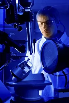
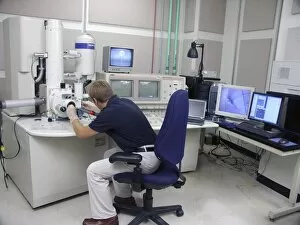
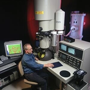
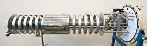
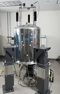
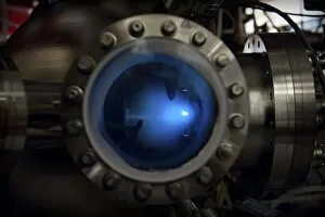
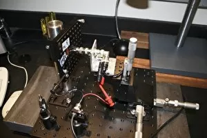
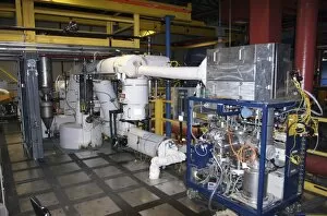
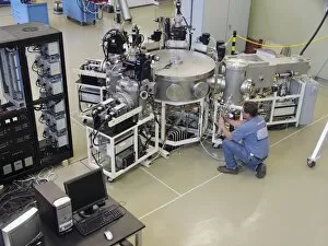
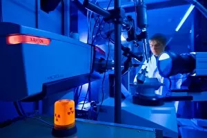
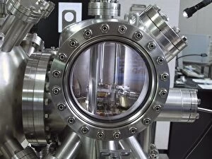
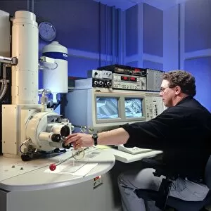
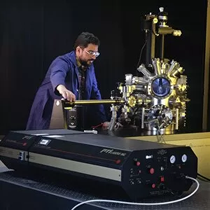
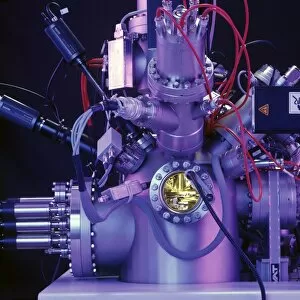
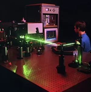
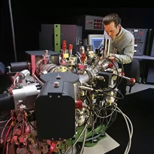
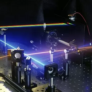
Characterization and measurement play a crucial role in various scientific fields, allowing researchers to gain valuable insights into the properties and behavior of materials. Advanced techniques such as X-ray crystallography (C016 / 3824), FE scanning electron microscopy (C016 / 3821), and Scanning transmission electron microscopy (C016 / 3815) enable scientists to visualize the atomic structure of materials with exceptional detail. For elemental analysis, the Rutherford backscattering spectrometer (C016 / 3834) provides precise measurements of composition and thickness. Meanwhile, Nuclear magnetic resonance spectrometer (C016 / 3830) allows for the study of molecular structures and dynamics by analyzing nuclear spin interactions. In manufacturing processes like pulse laser deposition apparatus (C016 / 3828), it is essential to measure thin film growth rates accurately. Photovoltaic cell testing equipment (C016 / 3829) ensures that solar cells meet efficiency standards before deployment. To investigate gas-phase reactions or analyze complex mixtures, scientists employ tools like Molecular beam mass spectrometers (C016/3825). These instruments offer high-resolution detection capabilities for identifying individual molecules based on their mass-to-charge ratio. Silicon cluster manufacturing tools (C016/3822) are utilized in nanotechnology research to create clusters with specific sizes for various applications. The X-ray crystallography instrument (CO16/3823) helps determine crystal structures by measuring diffraction patterns produced when X-rays interact with crystals. Furthermore, Scanning probe microscopy sample holders (CO16/3820), combined with Scanning Electron Microscopy (CO16/3816), allow researchers to investigate surface topography at nanoscale resolution while simultaneously obtaining compositional information about the sample.